Agilex hardware + optimization

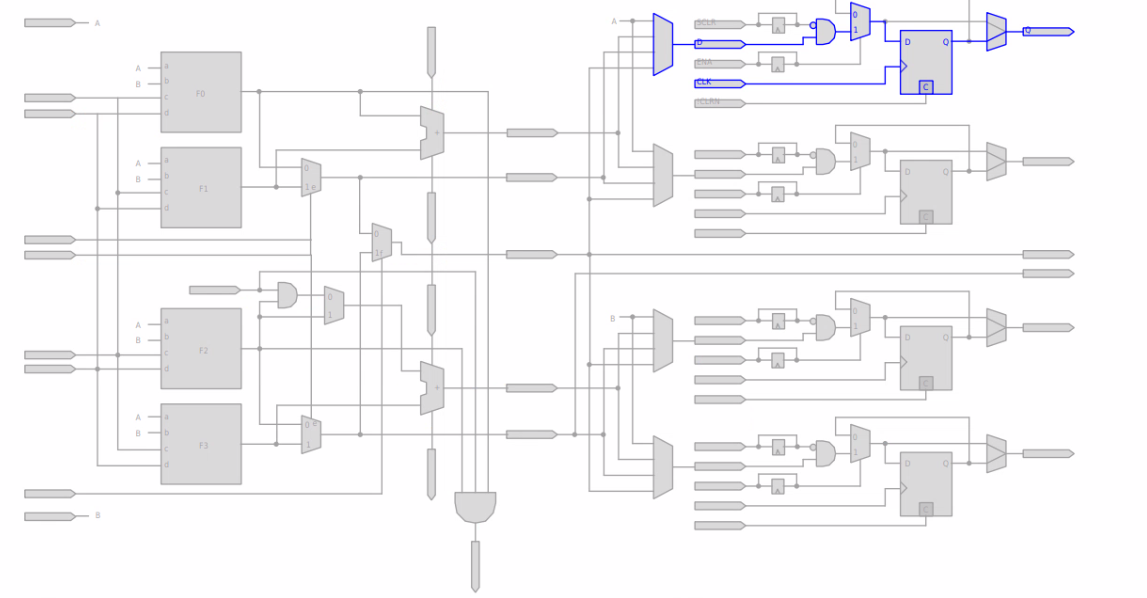
ALM
- configurable LUT
- combinations of 8 input signals to 4+4; 5+3; 5+4; 5+5; single 6 input LUT
- 8 input LUT extended mode - not all functions are supported. Multiplexers preferred.
- Adder with LUT combinations above
- 4 registers
- Differences/implications from other families
- Can pack 4-wide input functions per reg or pair of reg (Logic Element like)
- If everything were 6-input LUT optimised, ALUT vs reg resource usage may not follow
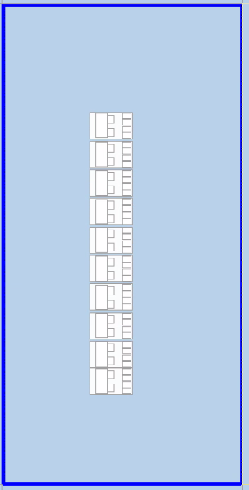
LAB
- block of 10 ALMs
- LAB wide ctrl signals
- 2x clk
- 2x clk_ph (delayed clocks)
- 2x clr (async)
- 2x clkena
- 1x synclr
- May be reconfigured as MLAB = 640b arranged as 32x20
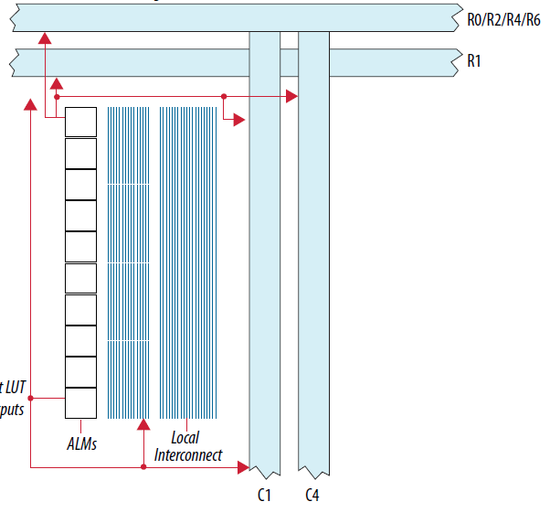
Routing
- local interconnect connects to different length wires (with different delays)
- Only really a consideration for tightly packed designs
- Evaluate usage with chip planner
Hyperflex registers
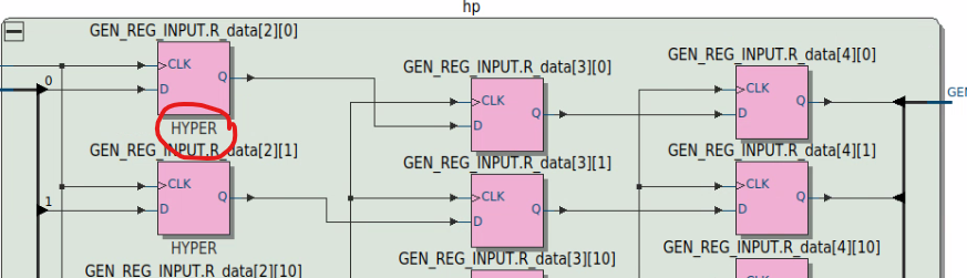
- Simple D type flops are distributed through the routing for Agilex devices.
- These have CLK, D, Q only - remove resets where feasible.
- I recommend you start with a no-reset mindset and add sync resets and async resets only where needed to guarantee startup behaviour
- The Quartus Prime Pro software has an excellent retimer and diagnosis tools to push registers back.
- I recommend including a variable latency register back at the output of a module to allow you to easily increase latency and allow the fitter to push the registers back into your design
- The Technology Map viewer identifies the hyperflex registers by
labelling them
HYPER - Turn on fast-forward in Synthesis settings or using
set_global_assignment -name FLOW_ENABLE_HYPER_RETIMER_FAST_FORWARD ONfor recommendations on how to reduce critical paths, and what the fmax could be.
Inference recommendations for RAM/ROM
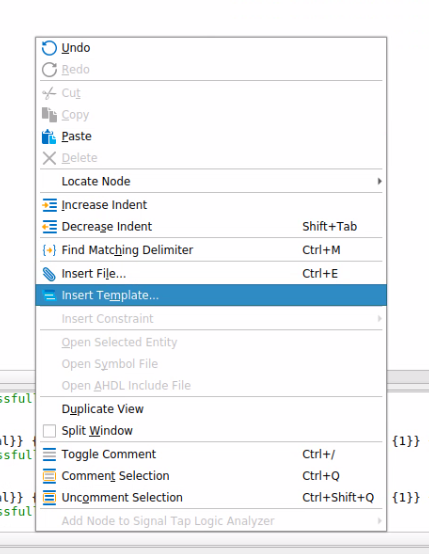
- Right click on Quartus text editor and select Inset Template to get examples of inference patters that work
- Use examples from the classic Advanced Synthesis Cookbook
- verify your low level building books map to hardware as you expect before reusing them
- Assert on read during write in simulation and stay with Quartus Prime can infer RAM with don’t-care rdw behaviour
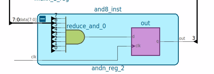
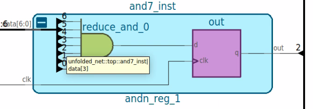
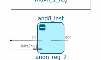
Netlist viewers
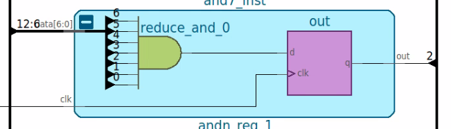
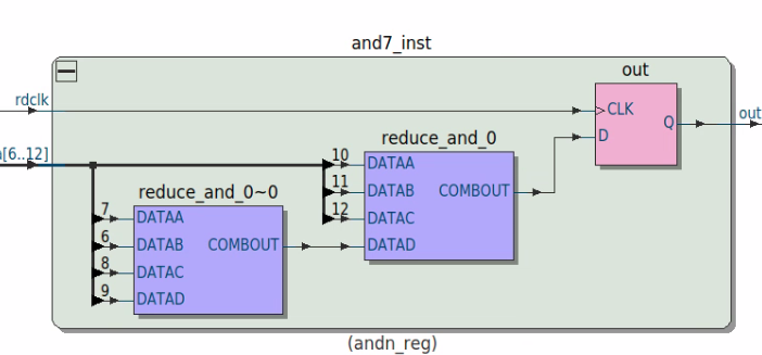
- Netlist viewers are available for multiple stages of compilation
- Elaborated = language extraction
- Swept = redundant logic removal
- Look at the Compilation Dashboard to see all available snapshots and netlist views
DSP / multiplier inference
- latency
- DSP blocks have input, output, 2xpipeline registers
- 4 cycles latency when all registers are enabled
- Not populating all registers impacts fmax
- Retimer can retime registers through DSP blocks
- DSP blocks have input, output, 2xpipeline registers
- Data type
- DSP blocks have native floating point support
- Using floating point types reduces fmax by ~18%
- tensor mode
- Agilex 5 introduces tensor mode - sum of products
- FP16 and INT8 supported
- Agilex 5 introduces tensor mode - sum of products
- Inference
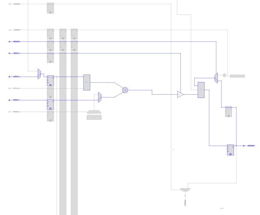
- some modes have complex inference models
- Use Insert template -> … -> Arithmetic as starting point
Performance estimation
- What’s possible on real-life designs
- Agilex 7 SIMT soft processor - 950MHz
- Agilex 7 FIR, FFT - 560MHz FFT, 900MHz FIR
- Agilex 7 opencores - 380 - 800MHz
- Agilex 3 opencores - 250MHz - 350MHz
- NB the opencores evaluations are performed on unmodified code - no optimization
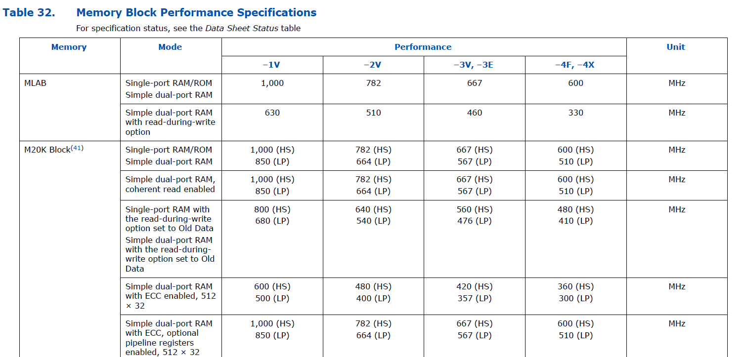
- Check datasheets for upper limit
Module level optimization
- Use assignments to reduce available resources to the fitter
set_instance_assignment -name MAX_LABScan be used to control number of LABS (=ALM*10)set_instance_assignment -name MAX_RAM_BLOCKS_M4Kcan be used to control number of M20K BRAMsset_instance_assignment -name MAX_BALANCING_DSP_BLOCKScan be used to control number of DSP blocks- The assignments may be applied to a module instance using
set_instance_assignmentor to the whole design usingset_global_assignment
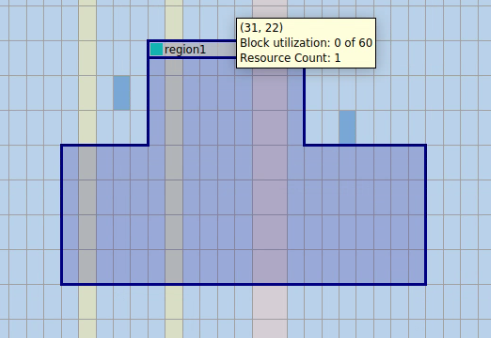
Use LogicLock to restrict usage to an area of the FPGA
Assignments -> Logic Lock Regions Window or Tools -> Chip Planner to draw regions
![logiclock]()
Assign logic by design entry hierarchy or Design Partition
